Introduction to Dam and Fill Encapsulation: Protecting Specific Components
Dam and fill encapsulation is an advanced material technique used in PCB manufacturing to protect sensitive components from moisture, dust, vibration, and chemical exposure. As the electronics industry pushes for ever-smaller footprints and higher reliability, safeguarding chips, sensors, and connectors with targeted encapsulation techniques is crucial. Choosing the right materials and proper process steps ensures components survive harsh environmental and mechanical conditions, supporting both performance and longevity. This article explores dam and fill encapsulation: protecting specific components, breaking down material selection, process sequences, real-world case studies, and actionable tips for superior PCB durability.
What is Dam and Fill Encapsulation?
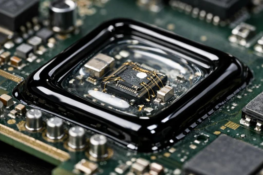
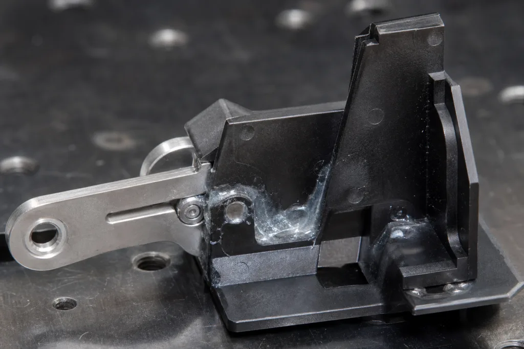
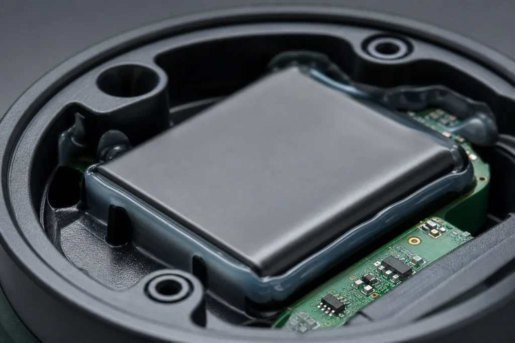
Dam and fill encapsulation combines two stages: a viscous “dam” forms a physical barrier around a sensitive area, while a lower-viscosity “fill” compound is dispensed inside this boundary. The dam confines the fill material, enabling precise coverage and preventing overflow onto adjacent circuits. This dual-layer technique locks out environmental hazards, cushioned mechanical stress, and secures delicate surfaces.
The Role of Dam in Component Protection
The dam uses a higher-viscosity polymer—typically an epoxy, silicone, or UV-cure formulation—applied around targeted PCB regions. It stands tall enough to contain the fill, serving as a fence to localize protection.
The Function of Fill in Encapsulation
The fill layer flows inside the dam, covering exposed surfaces, pinouts, and terminations. It cures to form a durable, cohesive shell that resists water ingress, dust, and impact.
Why Use Dam and Fill Encapsulation for Component Protection?
Dam and fill encapsulation is preferred over one-part pottings when manufacturers need topical precision, low-profile layering, and selective isolation of sensitive devices.
- Custom barriers mean better protection for high-risk spots—like wire bonds, MEMS sensors, and connectors.
- The method minimizes excess weight and does not interfere with thermal management or neighboring circuitry.
- It enables rework and inspection, since the encapsulated area is visually accessible and localized.
For PCBs in automotive, medical, and industrial settings, dam and fill helps manage reliability in tough conditions.
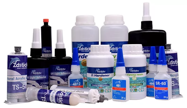
Choosing Suitable Materials for Dam and Fill Encapsulation
Material selection is the backbone of effective encapsulation. Engineers pick epoxy, silicone, or polyurethane systems based on substrate compatibility, cure speed, operating temperature, and resistance requirements. epoxy adhesives offer excellent mechanical strength and chemical resistance, while silicone excels in flexibility and thermal stability. Polyurethane blends are chosen for shock absorption and UV resilience.
Key Properties of Dam Materials
- Viscosity: Must form a robust wall that won’t collapse or slide during fill application.
- Cure Mechanism: UV-cure, heat-cure, and moisture-cure each offer specific benefits for assembly speed and reliability.
- Height and Shape Stability: The dam must retain its contour until the fill is added.
Ideal Fill Material Features
- Low viscosity ensures thorough coverage and self-leveling.
- Thermally conductive fillers combat heat buildup in power circuits.
- Dielectric strength protects against short circuits; see industry reviews on polyurethane structural adhesives for demanding uses.
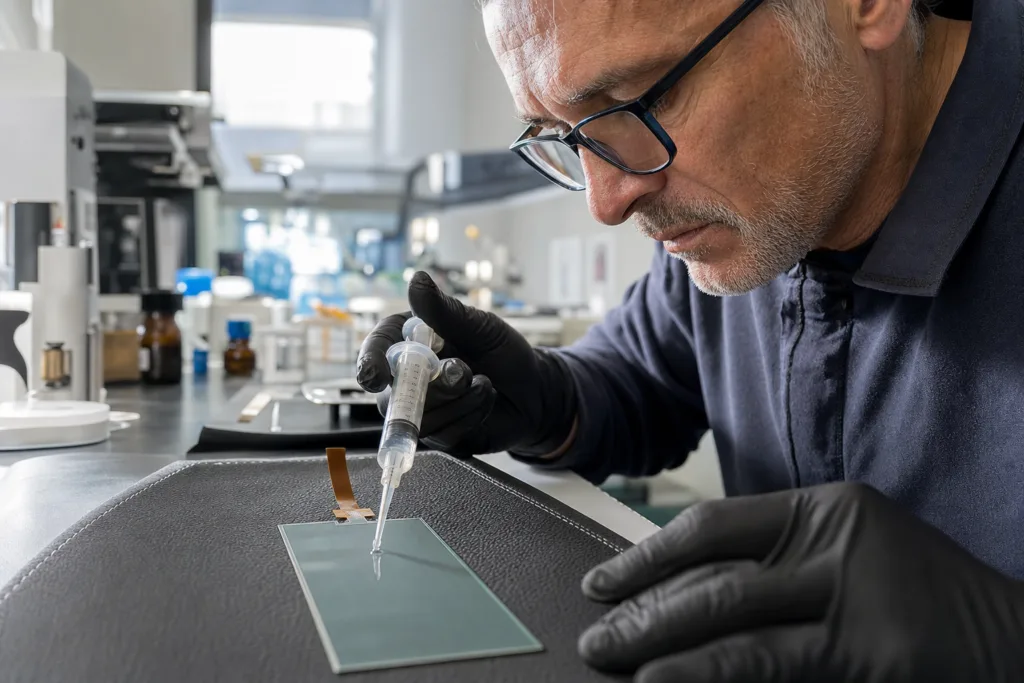
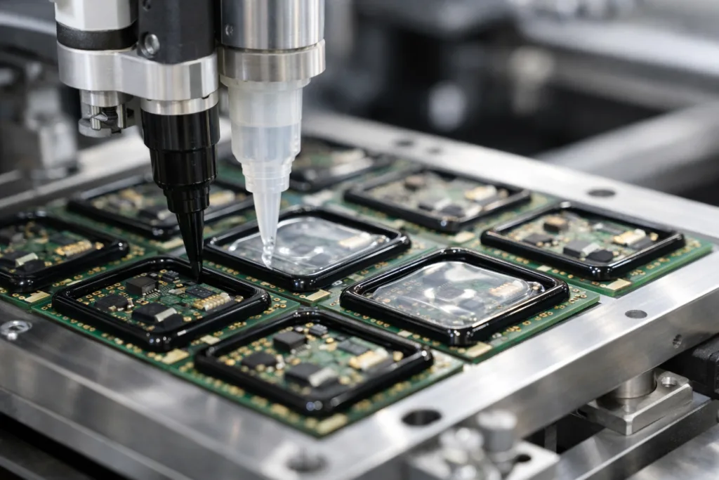
Process Steps for Successful Dam and Fill Encapsulation
Executing dam and fill requires careful sequencing:
- Surface Preparation: Clean and dry the PCB to enhance adhesion.
- Dam Application: Dispense a bead around the chosen area; cure as necessary (UV or heat).
- Fill Dispensing: Deposit fill inside the dam; allow flow and settle, then cure.
- Inspection: Check for uniform coverage and absence of air bubbles.
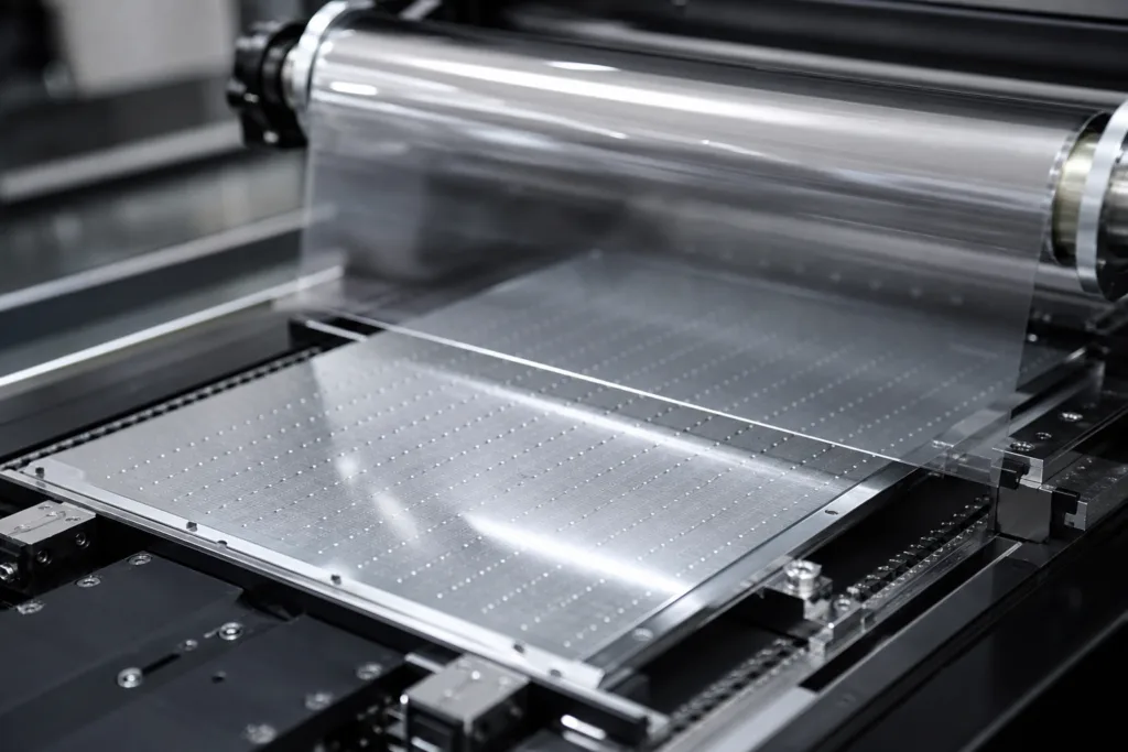
Automation and Quality Control
Modern PCB lines leverage robotic dispensing for tight repeatability. Machine vision checks dam height and fill uniformity, critical for high-volume production.
Comparing Dam and Fill Encapsulation with Other Protection Methods
| Protection Method | Coverage | Strengths | Limitations |
|---|---|---|---|
| Dam & Fill | Localized | Selective, visual, reworkable, minimal excess mass | May require advanced dispensing |
| Full Potting | Total | Maximum isolation, impact protection | Heavy, can trap heat, difficult for inspection |
| Conformal Coating | Surface-level | Lightweight, covers entire PCB | Limited mechanical barrier, not suited for wire bonds |
Case Studies: Effective Dam and Fill Encapsulation in PCB Manufacturing
In automotive sensor modules, targeted dam and fill encapsulation has extended life during thermal cycling and road vibration. For medical devices, precision encapsulation ensures biocompatible seals around MEMS microphones, enabling operation under sweat and humidity. Industrial controllers benefit from dam and fill at I/O connectors—allowing ruggedization without obstructing heat dissipation.
From ZDS Adhesive, an industrial adhesive manufacturer’s perspective, silicone-based dams coupled with thermal-conductive fills achieve stable performance between -40°C and +125°C, resist solvents, and easily pass moisture ingress testing. Key metrics include lap shear strength above 12 MPa, peel resistance, and consistent bond-line thickness below 1.5 mm.
Common Pitfalls and Troubleshooting Tips
Failure to control dam viscosity or allow appropriate cure time leads to fill leakage or voids. Humidity and contamination during filling cause bubbles, weakening the protective layer. Practical troubleshooting involves:
- Testing dam height and firmness before fill.
- Drying PCBs with gentle heat pre-encapsulation.
- Using vacuum-assisted fill dispensing for sensitive electronics.
- Verifying cleanliness with isopropyl alcohol before processing.
Tips for Ensuring Best Results During Dam and Fill Encapsulation
- Select dam material with cure speed that suits line velocity.
- Use pre-mixed, air-free fill compounds for high-value circuits.
- Monitor ambient conditions and humidity in the workspace.
- Inspect encapsulated areas under UV light for completeness.
- Spec out thermal cycling and chemical resistance in your material selection.
Consult resources like industrial adhesives for tailored recommendations. Always compare datasheets for compatibility and environmental safety.
Environmental and Mechanical Benefits of Dam and Fill Encapsulation
By focusing protection only where it’s needed, dam and fill prevents corrosion, shorts, and physical stress without adding bulk. Modern formulations offer fire retardancy, UV resistance, and minimal outgassing, making them ideal for mission-critical systems in EVs, medical wearables, and industrial controls. Reduced mass means improved cooling and easier future upgrades.
Dam and Fill Encapsulation: Protecting Specific Components
This technique is a go-to solution in 2026 for ensuring component-level survivability. It supports design flexibility, allowing engineers to tailor protection for high-value chips, connectors, or sensors. With robotic dispensing and smart materials, process repeatability and quality assurance are easier than ever.
Advancements in Dam and Fill Encapsulation Materials
Recent developments include UV-curable dams for instant barrier formation and low-trace, halogen-free fills meeting green electronics requirements. Nano-fillers enhance thermal conductivity, while latent curing agents optimize open time for complex layouts. These innovations push reliability even further in compact PCBs and wearables.
Conclusion: Key Takeaways for Component Protection

Dam and fill encapsulation: protecting specific components offers unmatched precision, durability, and environmental protection for modern electronics. Strategic material selection and process control make the difference between reliable operation and costly failures. As manufacturing evolves, this technique remains a cornerstone for selective, robust PCB safeguarding.
Frequently Asked Questions
What is dam and fill encapsulation in PCB manufacturing?
Dam and fill encapsulation involves creating a barrier (dam) around vulnerable components and filling that area with a protective material, securing the component against environmental impact and mechanical stress.
Which materials are best for dam and fill encapsulation?
Epoxt, silicone, and polyurethane are common. Choose based on electrical, mechanical, and thermal requirements—a careful review of datasheets is essential.
How do you ensure the dam doesn’t collapse during fill application?
Use high-viscosity dam materials that cure quickly and retain their shape, and verify height with machine vision or manual inspection before fill.
Can dam and fill encapsulation be automated?
Yes, robotic dispensing systems and automated vision inspection make this technique suitable for high-volume PCB production lines.
Is dam and fill encapsulation reworkable?
Typically, yes. Unlike full potting, dam and fill concentrates protection so local rework and assembly inspection remain feasible.
How does dam and fill compare to conformal coating?
Dam and fill provides strong mechanical and environmental barriers for specific components; conformal coating is lighter, but offers less targeted protection.
Related Reading
- Which PCB Protection Method Wins? Potting vs. Conformal Coating Unpacked
- Uncover Hidden Strengths of Single-Component Epoxies with Latent Curing Agents
- How B-Stage Epoxies Optimize Manufacturing: Storage, Processing, and Reliability Tips
- Master Thermal Management: 13 Real-World Techniques for Large Epoxy Castings
- Breakthrough Dual-Cure Systems for Shadow Area Failures: Heat & Moisture Back UV Success