E-mail

Sale01@epoxyresinfactory.com
sale04@epoxyresinfactory.com

Contact

Tel: 86-755-84875752
Fax: 86-755-84875750

Address

4F,Longyuntong Building, No. 164-5 Pengda Road, Longgang District, Shenzhen

Semiconductor Packaging

Depicts a professional assembly environment for GaN and SiC power modules, emphasizing the advanced materials and process controls used in third generation semiconductors.

7 Critical Advances in Packaging Materials for GaN and SiC (3rd Gen Semi): Industry Solutions & Trends

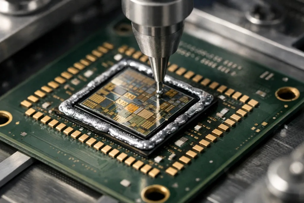
Introduction: The New Frontier of Packaging Materials for GaN and SiC (3rd Gen Semi) Gallium Nitride (GaN) and Silicon Carbide (SiC) are leading the charge in third generation semiconductors, signaling a shift in how engineers approach packaging materials for power electronics. These wide-bandgap materials outperform traditional silicon in switching speed, efficiency, and power density, but […]

7 Critical Advances in Packaging Materials for GaN and SiC (3rd Gen Semi): Industry Solutions & Trends Read More »

A professional view of semiconductor packages with adhesives applied, featuring MSL (Moisture Sensitivity Level) labels indicating protective handling procedures.

Master Moisture Sensitivity: 9 Critical Steps for Adhesive Selection in Semiconductor Packaging

Understanding Moisture Sensitivity, Adhesive Selection: The Foundation of Reliable Semiconductor Packaging Moisture Sensitivity Level (MSL) is a critical factor in semiconductor packaging—one that directly guides adhesive selection and determines long-term device reliability. This article explores how closely moisture sensitivity, adhesive chemistry, and process controls are connected. Failing to align adhesives to a component’s MSL can

Master Moisture Sensitivity: 9 Critical Steps for Adhesive Selection in Semiconductor Packaging Read More »

A laboratory setting displays a clear silicone encapsulant covering an LED chip, highlighting its optical clarity and refractive behavior in modern LED packaging.

How Silicone’s Refractive Index Powers the Next Generation of LED Packaging

Understanding Silicone Refractive Index in LED Packaging When it comes to LED packaging, the choice of encapsulant material just might be the unsung hero behind device efficiency and reliability. Silicone, a trusted performer in many optoelectronic applications, stands out largely because of its refractive index — a property dictating how light moves from the LED

How Silicone’s Refractive Index Powers the Next Generation of LED Packaging Read More »

A photo-realistic scene showing IGBT/MOSFET modules surrounded by high-temp silicone encapsulant under well-lit factory conditions, highlighting technical application.

The Complete 2026 Guide: How High-Temp Encapsulants Protect Power Module Reliability for IGBT/MOSFET

Introduction: The Role of High-Temp Encapsulants for Power Modules (IGBT/MOSFET) Power electronics drive modern technology—from electric vehicles to renewable energy systems. As these systems push ever-higher voltages and power densities, the thermal and environmental demands on their critical components multiply. This is especially true for Insulated-Gate Bipolar Transistors (IGBTs) and Metal-Oxide-Semiconductor Field-Effect Transistors (MOSFETs), which

The Complete 2026 Guide: How High-Temp Encapsulants Protect Power Module Reliability for IGBT/MOSFET Read More »

This image captures the intricate process of applying EMI shielding pastes to SiP structures, emphasizing the importance of precision in preventing electromagnetic interference in compact electronic packaging.

How EMI Shielding Pastes Empower Next-Gen System-in-Package (SiP) Electronics

Introduction: Why EMI Shielding Pastes Matter in System-in-Package (SiP) Electronics Electromagnetic interference, commonly known as EMI, poses a major threat to the functionality and reliability of compact electronic devices. As modern gadgets become smaller, faster, and more densely packed thanks to System-in-Package (SiP) integration, the need for robust EMI shielding solutions has never been greater.

How EMI Shielding Pastes Empower Next-Gen System-in-Package (SiP) Electronics Read More »

A detailed scene of wafer dicing with advanced temporary bonding tape applied, capturing industrial precision and cleanroom standards.

Temporary Bonding Tapes for Wafer Dicing: 9 Game-Changing Insights for Fewer Production Failures

Introduction to Temporary Bonding Tapes for Wafer Dicing Temporary bonding tapes for wafer dicing play a vital role in the semiconductor industry, enabling the safe and accurate processing of wafer substrates. These specialized tapes anchor delicate wafers to dicing frames, protecting their integrity during high-precision cutting and minimizing chipping or cracking. As the semiconductor landscape

Temporary Bonding Tapes for Wafer Dicing: 9 Game-Changing Insights for Fewer Production Failures Read More »

This image presents capillary underfill being applied to flip-chip packaging inside a modern cleanroom, highlighting the adhesive flow under a semiconductor die.

Capillary Underfill for Flip-Chip Packaging: 12 Proven Steps to Reliable Joints in 2026

Introduction to Capillary Underfill Process for Flip-Chip Packaging The capillary underfill process for flip-chip packaging is a fundamental technique in modern semiconductor assembly. When manufacturing advanced microelectronic devices, creating reliable electrical and mechanical connections is crucial. Flip-chip packaging enables direct connection of a semiconductor die to the substrate, but it comes with significant mechanical and

Capillary Underfill for Flip-Chip Packaging: 12 Proven Steps to Reliable Joints in 2026 Read More »

A technician uses industrial tools to carefully apply a soft encapsulant to a MEMS sensor, which illustrates the attention required for minimizing mechanical stress.

Low Stress Encapsulants for MEMS Sensors: 12 Transformative Tips for Reliable Packaging

Introduction: Why Low Stress Encapsulants Matter for MEMS Sensors Micro-Electromechanical Systems (MEMS) sensors drive countless innovations in automotive, medical, industrial, and consumer electronics. The protection and performance of these sensors depend heavily on encapsulation—a process that shields delicate components from moisture, dust, chemicals, and mechanical forces. However, conventional encapsulants often introduce unwanted stress, leading to

Low Stress Encapsulants for MEMS Sensors: 12 Transformative Tips for Reliable Packaging Read More »

This image depicts the manufacturing process of cob (chip on board) glob top encapsulation, focusing on precision equipment and the critical moment of material application for high-reliability platforms.

COB Glob Top Encapsulation: 13 Proven Advantages & Best Practices for 2026

Understanding COB (Chip on Board) Glob Top Encapsulation COB (Chip on Board) glob top encapsulation is a crucial process for protecting delicate semiconductor dies mounted directly on printed circuit boards (PCBs). This guide demystifies COB, glob top encapsulation chemistry, and practical deployment, focusing on durability, performance, and the impact of material selection. As COB technologies

COB Glob Top Encapsulation: 13 Proven Advantages & Best Practices for 2026 Read More »

A detailed view depicts silver-filled adhesive bonding a semiconductor die to a substrate, emphasizing both conductivity and heat management requirements.

Mastering Die Attach Adhesives: 9 Ways Conductivity & Heat Management Transform Electronics in 2026

Introduction: Why Die Attach Adhesives Must Balance Conductivity and Heat Die attach adhesives, a cornerstone of semiconductor assembly, play a double role: ensuring strong bonds and managing both heat and electrical flow. Especially in power electronics and high-frequency devices, the choice of adhesive shapes device reliability and efficiency. This article breaks down how thermal conductivity

Mastering Die Attach Adhesives: 9 Ways Conductivity & Heat Management Transform Electronics in 2026 Read More »

Scroll to Top

💬 Let’s Build Something Strong Together

Have a project in mind or need a reliable adhesive solution?
Our experts are ready to help — just drop us a message!

✅ Tailor-made adhesive formulations
✅ Fast lead times & global shipping
✅ Trusted by manufacturers worldwide

📩 Leave your details and let’s make it happen.
We’ll get back to you within 24 hours.

Look out for emails from @zdschemical.com.

ZDSâ„¢ Adhesive manufacturer

Free Access to Test Samples or Quote

Response time as fast as 30 minutes.

📧 Prefer a fast reply? Email us directly at: Sale01@epoxyresinfactory.com
ZDS Adhesive Manufacturer

Not Sure Which Adhesive Fits?

Our engineers are ready to help. Drop us a message.

📧 Prefer a fast reply? Email us directly at: Sale01@epoxyresinfactory.com