Introduction: The New Frontier of Packaging Materials for GaN and SiC (3rd Gen Semi)
Gallium Nitride (GaN) and Silicon Carbide (SiC) are leading the charge in third generation semiconductors, signaling a shift in how engineers approach packaging materials for power electronics. These wide-bandgap materials outperform traditional silicon in switching speed, efficiency, and power density, but their unique properties create urgent demands for specialized packaging designs. This article explores the evolving landscape of packaging materials for GaN and SiC (3rd Gen Semi), examining how innovations in thermal management, electrical performance, and process reliability shape best practices and push industry standards.
| Material | Thermal Conductivity (W/m·K) | Electrical Properties | Typical Applications |
|---|---|---|---|
| Ceramic Substrates | 25–180 | High insulation | Power modules, RF devices |
| Epoxy Mold Compounds | 0.6–2 | Good barrier | Encapsulation, chip protection |
| Silicone Encapsulants | 0.2–4 | Flexible, moisture resistance | Power chips, LED packaging |
| Solder Alloys | 40–60 | Conductive | Die attach, interconnect |
| Thermal Greases/Pads | 1–15 | N/A | Heat dissipation interface |
The Role of Packaging Materials in GaN and SiC Power Devices
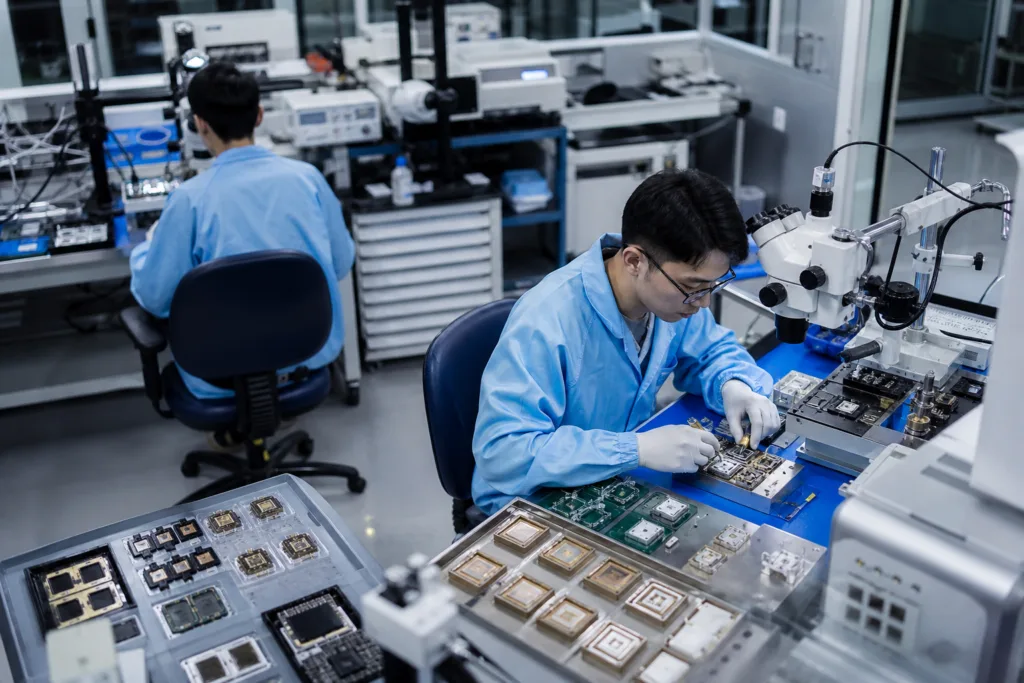
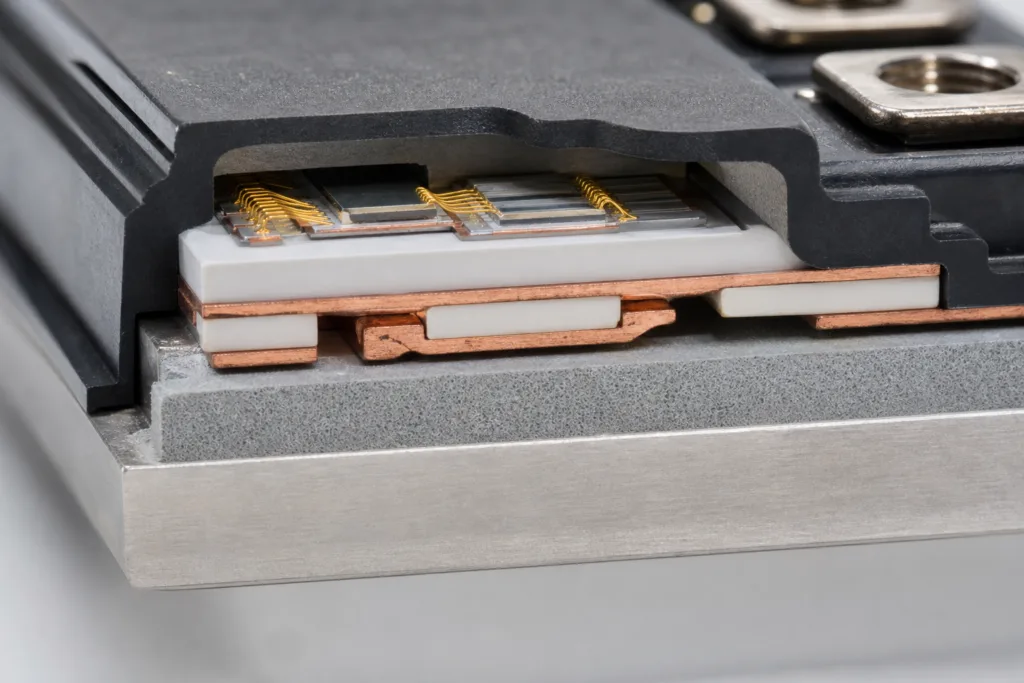
Packaging materials serve as the silent workhorses of device reliability in next-generation semiconductors. As GaN and SiC push power density higher, thermal management and electrical insulation become paramount. Ceramic substrates, such as AlN and Si3N4, offer superior heat sinking, while organic mold compounds must resist thermal stress and minimize moisture intrusion. This complex balancing act demands advanced materials and production precision. For further details, see The Complete 2026 Guide: How High-Temp Encapsulants Protect Power Module Reliability for IGBT/MOSFET.
Challenges Unique to GaN and SiC Semiconductor Packaging
Compared to silicon, GaN and SiC power devices operate at far higher voltages, frequencies, and temperatures. Packaging materials must address:
- Thermal runaway prevention: Efficient heat spreading to avoid device failure.
- Electrical insulation: Maintaining isolation at higher voltage gradients.
- Mechanical stress: Accommodating CTE mismatch and cyclical loading.
- Moisture and contamination resistance: Ensuring long-term reliability.
Failure to manage these factors often results in premature breakdowns. According to industry specialists, even slight imperfections in packaging can degrade performance, underscoring the need for rigorous material selection.
Comparing Traditional Silicon Packaging with GaN and SiC Solutions
Silicon power modules use familiar mold compounds, copper leadframes, and basic epoxy underfills. In contrast, 3rd Generation semi devices leverage:
- High-temperature ceramic substrates for superior thermal conductivity
- Advanced die attach adhesives or solders for robust heat transfer
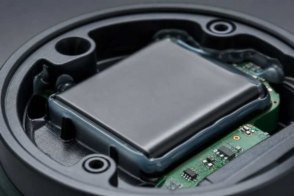
- Flexible, low-stress encapsulants to combat thermal expansion
- Enhanced conformal coatings for moisture barrier
| Feature | Silicon | GaN/SiC |
|---|---|---|
| Max Operating Temp (°C) | 150 | 200–350 |
| Switching Speed | Moderate | Ultra-fast |
| Packaging Complexity | Standard | Advanced |
| Thermal Management | Basic | Critical |
Material Innovations: Ceramic Substrates, Encapsulants, and Thermal Pads
Ceramic substrates (aluminum nitride, silicon nitride) now set the bar for heat sinking and insulation, leaving FR4 and simple mold compounds behind. Epoxy and silicone encapsulants are engineered for low stress and thermal cycling stability. Thermally conductive pads bridge the gap between chip and heatsink, reducing junction temperatures.
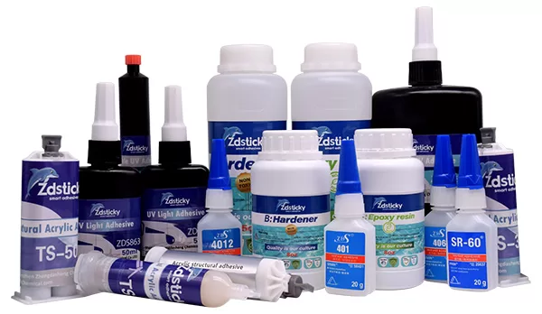
Recently, ZDS Adhesive, an industrial adhesive manufacturer, demonstrated that low-stress silicone gels enhance module resilience under cyclic thermal loads and reduce mechanical failures by 32% when tested to 5000 cycles (–40°C to 150°C). The choice of encapsulant hinges on both modulus and cure mechanism, especially for sensitive GaN and SiC power assemblies. You can learn more about how these silicone gels perform in Innovative Silicone Gel Solutions: How to Protect Metal Components from Stress Damage.
Best Practices: Selecting Packaging Materials for GaN and SiC Devices
When engineering wide-bandgap power modules, use a decision checklist based on:
- Thermal conductivity (choose ≥ 3 W/m·K for high power)
- Electrical insulation (dielectric strength ≥ 20 kV/mm)
- Low modulus for stress reduction (especially under cycling)
- Moisture resistance (water absorption < 0.2%)
- Cure speed and process window (match to production volumes)
- Adhesion to ceramics/metals (surface energy, compatibility)
Material compatibility testing—lap shear, thermal cycling, humidity aging—should always precede full-scale deployment on assembly lines.
Thermal Management: Key to Power Module Reliability
Efficient thermal management is non-negotiable for GaN and SiC. Heat must flow through substrates, encapsulants, and thermal interface materials seamlessly. Poor dissipation increases junction temperatures and shortens device life. Industry leaders recommend integrating high-conductivity ceramics, optimizing the thickness of die attach layers (thin, uniform bond lines), and leveraging advanced pads and greases. For practical assembly tips, visit Breakthrough Insights: Thermal Grease vs. Thermal Pads—2026 Performance Comparison for Heat Dissipation.
Moisture Sensitivity and Reliability Concerns in Packaging Materials for GaN and SiC (3rd Gen Semi)
Moisture poses a hidden threat to packaging materials, causing corrosion, delamination, and electrical leakage. Selecting formulations with high barrier properties and regularly validating with humidity aging tests are crucial. Modern encapsulants incorporate silane coupling agents to improve adhesion and resist water absorption. Manufacturers now track moisture sensitivity level (MSL) as a critical reliability metric.
Die Attach Adhesives and Solder Choices for GaN and SiC Packaging
Die attach technology is rapidly evolving. Conductive epoxies and high-melting solders have become preferred options for GaN and SiC, balancing thermal transfer and mechanical compliance. Silver-filled adhesives, Sn-Ag-based solders, and pressureless sintering methods each offer distinct advantages. The ideal choice hinges on module power rating, substrate compatibility, and expected thermal cycles.
Case Study: Automotive Power Modules
Automotive traction inverters have adopted SiC power modules for their ability to handle high voltages (>1200V) and high switching speeds. Packaging materials must withstand vibration, shock, and salt spray, while delivering consistent thermal and electrical performance. By switching to advanced encapsulants and ceramic substrates, one EV OEM reduced module failure rates by 25% over two years.
Emerging Technologies: Low-Stress Encapsulants and Next-Gen Coatings
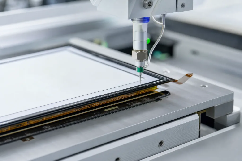
Next-generation packaging focuses on low-shrinkage, low-stress, and high-barrier materials. UV-curable gels, hybrid epoxies, and conformal coatings are now tailored to address rapid thermal cycling and harsh environments. Recent developments have shown that advanced UV adhesives improve alignment precision in automotive and power modules.
Improving Assembly Processes for GaN and SiC Devices
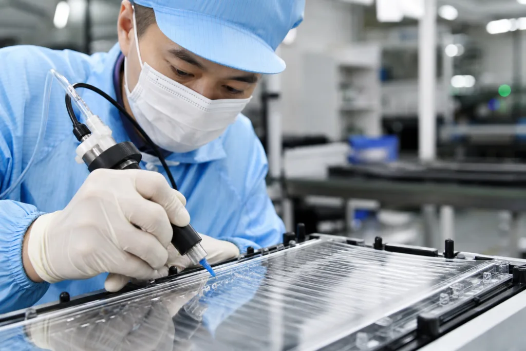
From an assembly engineer’s viewpoint, material selection is only part of the equation. Process controls—pot life, open time, fixture speed, cure profile—determine final product integrity. Operators must ensure the cure mechanism matches the thermal profile of the device to prevent voids and delamination. Regular process validation ensures consistency, particularly for high-value power modules.
Testing and Validation: Ensuring Packaging Performance in Wide-Bandgap Semiconductors
Reliability testing for GaN and SiC packaging includes:
- Thermal cycling (–40°C to 150°C, 1000–5000 cycles)
- Humidity aging (85°C/85% RH, 1000+ hrs)
- Lap shear and peel tests (substrate bonding strength)
- Voltage breakdown (dielectric withstand)
Only by meeting stringent test parameters can assemblies withstand real-world operational stresses.
Future Trends: Packaging Materials for GaN and SiC (3rd Gen Semi)
Industry forecasts point to rising adoption of hybrid materials—ceramic-organic blends, nano-enhanced encapsulants, and self-healing coatings. Artificial intelligence models now optimize process parameters in real-time, predicting failure modes before they occur. As electric vehicles and renewable energy expand, packaging reliability and efficiency will drive competitiveness.
Conclusion: Transforming Power Electronics with Innovative Packaging Materials

GaN and SiC are reshaping power electronics, demanding packaging solutions that outperform legacy silicon designs. Innovations in substrate materials, encapsulants, die attach adhesives, and thermal interface compounds are central to maximizing device reliability and efficiency. For engineers and manufacturers, mastering selection and process control of packaging materials for GaN and SiC (3rd Gen Semi) makes the difference between routine failures and world-class performance. As technology evolves, those who adapt to new material advances will set the pace for the industry.
Frequently Asked Questions
Why are packaging materials so critical for GaN and SiC devices?
GaN and SiC operate at higher temperatures and voltages than silicon, making advanced packaging essential for heat dissipation, electrical insulation, and protection from environmental factors.
What makes ceramic substrates preferred in GaN and SiC power modules?
Ceramic substrates offer superior thermal conductivity and electrical insulation, supporting higher power densities and improved reliability, especially under tough operating conditions.
How can moisture sensitivity affect GaN and SiC device reliability?
Excess moisture can cause corrosion and delamination in packaging materials. Using high-barrier encapsulants and rigorous MSL testing reduces failures linked to humidity exposure.
What testing should be performed for packaging reliability?
Key tests include thermal cycling, humidity aging, lap shear, peel, and voltage breakdown, all critical for verifying long-term performance in demanding applications.
How do die attach adhesives compare to solder for GaN and SiC modules?
Conductive epoxy adhesives are often more flexible and can absorb thermal stress, while solder provides superior thermal and electrical conduction. Selection depends on application needs.
What major trends are shaping packaging materials for GaN and SiC in 2026?
Hybrid materials, nano-enhanced additives, UV-curable gels, and AI-driven process optimization are key trends improving packaging reliability and efficiency for wide-bandgap semiconductors.
Related Reading
- Learn the 9 Critical Steps for Moisture Sensitivity in Semiconductor Packaging Adhesives
- Discover How to Balance Conductivity and Heat Management with Die Attach Adhesives in 2026
- Unlock Reliable Structural Bonds in Industry with High-Strength Epoxy Adhesives
- Achieve Reliable Flip-Chip Joints with 12 Proven Steps Using Capillary Underfill
- Find Real-World Advantages with Thermal Epoxy vs Softer Thermal Materials: Application Guide