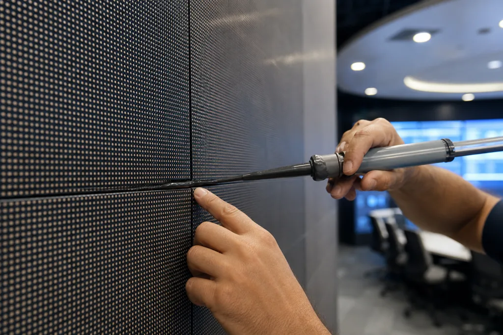
Introduction to UV Nano-Imprint Lithography for Touch Screens
Touch screen technology continues to shape the way we interact with devices, from smartphones to automotive displays. Among the advanced manufacturing processes propelling this innovation is UV nano-imprint lithography. This technique uses ultraviolet light and precisely shaped molds to pattern surfaces at the nanoscale, transforming how touch screens are built. Compared to traditional lithography, UV nano-imprint lithography brings higher resolution, better efficiency, and the potential for significant cost reduction. As the demand for larger, clearer, and more responsive screens grows, understanding this breakthrough has never been more important for engineers, manufacturers, and technology enthusiasts.
What Is UV Nano-Imprint Lithography?
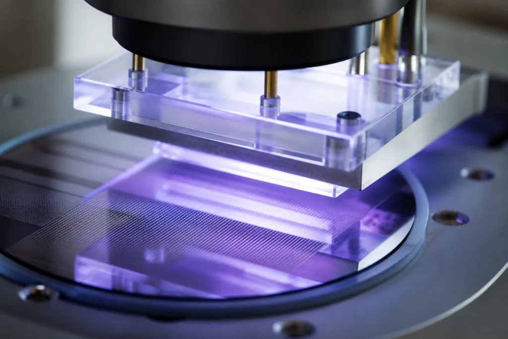
At its core, UV nano-imprint lithography is a method of transferring extremely fine patterns onto a substrate using a mold and ultraviolet (UV) light. The process involves placing a liquid photopolymer on the target surface, pressing a patterned stamp into the liquid, and curing it with UV light to create a permanent nano-structured pattern. This accuracy enables the fabrication of intricate conductive or insulating pathways essential for responsive touch screens.
How UV Nano-Imprint Lithography Works
The UV nano-imprint lithography process unfolds in several key steps:
- Application of a UV-curable resist (a type of photopolymer) onto the substrate surface.
- Alignment and pressing of a transparent, nano-patterned mold onto the resist layer.
- Exposure to UV light, which hardens the resist, conforming exactly to the mold’s shape.
- Separation of the mold, leaving behind a nano-scale relief pattern ready for further processing.
This procedure can be repeated rapidly on multiple substrates, supporting high-throughput manufacturing lines. Advanced liquid dispensing machines play a vital role in this workflow, ensuring accurate material placement while minimizing waste. For an expert’s look at configuring dispensing equipment for these adhesives, see How Liquid Dispensing Machines Must Be Configured for Epoxy, Silicone, and UV Adhesive Applications.
Why Is UV Nano-Imprint Lithography Ideal for Touch Screens?
Touch screens require patterns at the nanometer scale to detect minute touches and gestures. UV nano-imprint lithography allows manufacturers to produce remarkably consistent structures under 100 nanometers, leading to better capacitive touch performance and higher display resolution. The resulting improvements in signal clarity and reduced interference elevate the overall user experience, meeting consumer expectations for smooth, precise interactions.
Comparing UV Nano-Imprint Lithography to Traditional Lithography
| Main Feature | Traditional Photolithography | UV Nano-Imprint Lithography |
|---|---|---|
| Pattern Resolution | ~30–100 nm (limited by light diffraction) | <10 nm (mold-defined, not light-limited) |
| Process Complexity | Many steps, complex alignment | Simpler, fewer steps, direct patterning |
| Material Costs | High (photoresists, masks, processing) | Lower (reusable molds, less waste) |
| Production Speed | Moderate to slow | Rapid (high-throughput possible) |
| Equipment Costs | Very high (stepper/scanner required) | Lower (simpler exposure unit) |
UV nano-imprint lithography stands out in its ability to achieve sharper patterns at lower costs and with enhanced throughput, especially important for large-format or curved screens.
Key Advantages of UV Nano-Imprint Lithography in Touch Screen Production
- Unparalleled pattern precision: Sub-20 nm accuracy, essential for responsive touch interfaces.
- Cost-effectiveness: Reusable molds reduce consumable costs; fewer steps minimize labor and energy use.
- Scalability: Adapts to both glass and flexible plastic substrates, suitable for smartphones, tablets, and automotive displays.
- Compatibility: Integrates with advanced adhesives and optical bonding strategies for seamless, distortion-free screens. Explore more about Choosing the Right Optical Bonding Method: OCR vs. OCA for Modern Automotive Curved Displays for deeper insight.
- Environmental efficiency: Less chemical waste and lower VOC emissions compared to some older processes.
Recent Breakthroughs in UV Nano-Imprint Lithography
In the past two years, several advancements have accelerated adoption in the touch screen industry:
- Flexible and curved patterning: Improved mold materials support wraps and bends for next-generation displays.
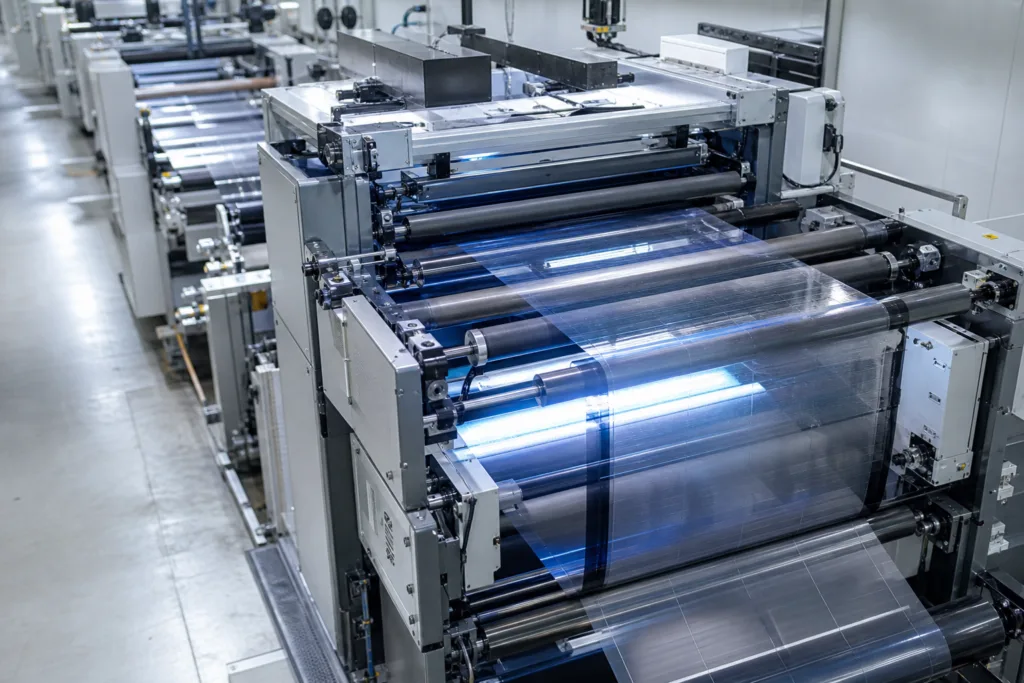
- High-throughput systems: Integration with roll-to-roll manufacturing drastically increases production speed.
- Material innovations: UV-curable resins with lower shrinkage and higher transparency extend usable device lifetimes.
- Integration with smart adhesives: Use of gap-filling and clear adhesives guarantees defect-free optics and long-term durability. Learn how modern gap filling adhesives are game changers for commercial video walls.
Challenges in Adopting UV Nano-Imprint Lithography
Despite the benefits, some barriers remain:
- Mold durability: Molds must withstand repeated cycles without losing fidelity, especially with harder substrates.
- Defect control: Dust or debris during imprinting can create unwanted flaws; cleanroom standards are critical.
- Alignment precision: Multi-layered touch panels require perfect overlay to avoid ghost touches or signal loss.
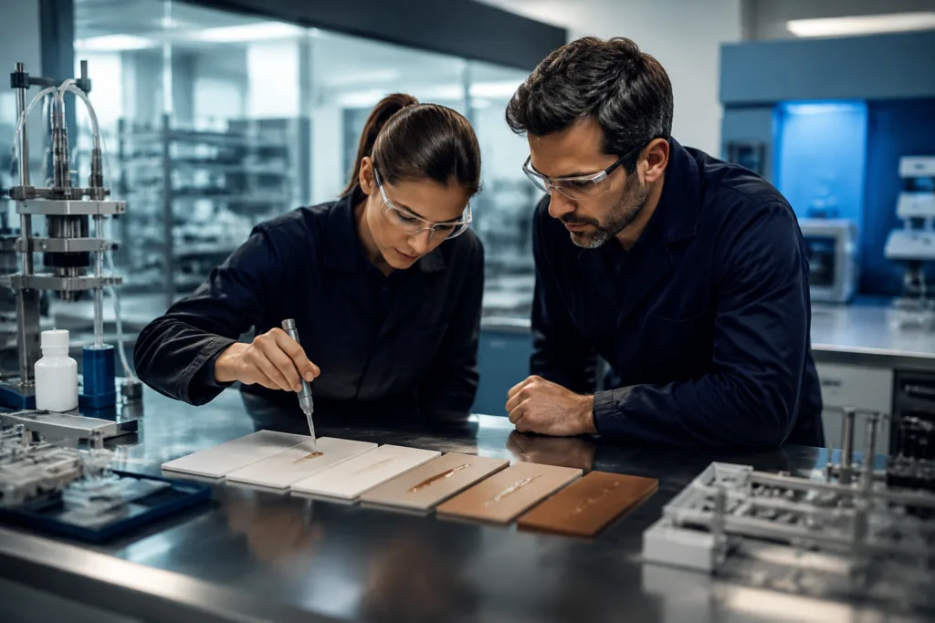
- Materials compatibility: Matching photopolymers, substrates, and adhesives demands careful testing.
UV Nano-Imprint Lithography for Touch Screens
Modern touch screens are multi-layered composites. Nano-imprint lithography exactly patterns functional and decorative layers—including transparent electrode grids, micro-lenses, and anti-fingerprint surfaces—by:
- Forming capacitive sensor structures with nanometer control
- Defining conductive traces for reduced signal crosstalk
- Imprinting surface texturing that repels fingerprints and glare
Each feature translates to a more satisfying user experience and greater display reliability.
Enhancing Precision and Efficiency in Manufacturing
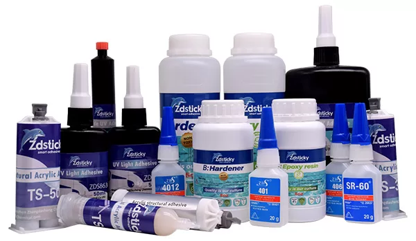
UV nano-imprint lithography increases efficiency by cutting down on processing steps and speeding up cycle times. Thanks to single-exposure patterning, manufacturing plants produce more screens with tighter tolerances and less waste. Using advanced adhesives for secure, distortion-free bonding—a specialty for ZDS Adhesive, an industrial adhesive manufacturer—brings further performance benefits and reduces post-production failures.
Impact on User Experience and Display Quality
Finer electrode grids mean sharper images, smoother touch recognition, and less visual noise. UV nano-imprinted surfaces can also support anti-glare and anti-smudge features. Whether it’s minimizing parallax errors on automotive clusters or making mobile screens clearer in sunlight, these innovations prioritize real-world usability.
Cost Reductions with UV Nano-Imprint Lithography
By enabling batch processing and reusable molds, UV nano-imprint lithography lowers per-unit costs even as devices become more advanced. Less material waste and reduced energy demands further add to factories’ bottom lines. For cost-sensitive sectors, like infotainment systems or entry-level smartphones, these savings are transformative.
Comparison: UV Nano-Imprint Lithography vs. Other Emerging Methods
| Method | Feature Size Limit | Throughput | Cost | Application Fit |
|---|---|---|---|---|
| UV Nano-Imprint Lithography | <10 nm | High | Low-medium | Large, curved, flexible screens |
| Inkjet Printing | ~10–20 μm | Moderate | Low | Simple/low-res patterning |
| Laser Direct Structuring | ~1 μm | Low | Medium-high | Prototyping |
Surface Treatment and Material Synergy
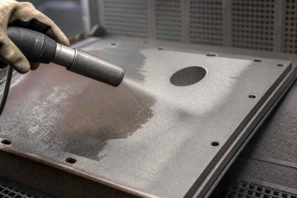
Optimal bonding and patterning rely on perfectly prepped surfaces. Plasma or corona treatments can raise surface energy, improving uniformity and curing. For a technical breakdown between these two popular methods, explore Plasma vs. Corona Treatment: Which Industrial Surface Process Wins in 2026?.
Advanced Adhesives in Touch Screen Assembly
Improved adhesives now complement nano-imprinted layers, especially in complex component stacks. Criteria for selection include optical clarity, low shrinkage, and rapid UV/thermal cure schedules. When used alongside nano-imprinted circuits, modern adhesives eliminate bubbles, lower scrap rates, and extend operating lifetimes.
Scalability and Integration with Modern Lines
UV nano-imprint lithography is increasingly paired with automated handling and vision systems for mass production. As panel sizes grow, ensuring registration accuracy across substrates up to 1 meter or more is key. Emerging roll-to-roll lines now apply this process rapidly to flexible and curved film, accelerating the rollout of new screen formats.
Applications Beyond Consumer Devices
This technology isn’t limited to phones and tablets. It’s critical in vehicle instrument clusters, interactive kiosks, industrial equipment, and even advanced medical displays where hygiene and durability are paramount. Antimicrobial nano-textures, for instance, can be patterned directly during imprint to keep screens cleaner for longer.
Environmental Considerations
Reducing chemical use and emissions is a major goal in modern fabrication. UV nano-imprint lithography’s minimal use of VOC-generating chemicals and recyclability of key components helps flatten the environmental footprint—even as production scales up to millions of units annually.
Future Trends and Industry Prospects
Looking ahead, we can expect further breakthroughs: hybrid approaches with atomic layer deposition, multi-level nano-structuring for richer haptics, and even smarter integration with embedded sensors. Touch screen markets—especially automotive and large-format signage—are likely to see cost and performance benefits escalate as the technology matures.
Conclusion: Is UV Nano-Imprint Lithography the Future of Touch Screens?
UV nano-imprint lithography is reshaping the economics and performance envelope of touch screen manufacturing. Its capacity for ultra-fine patterning, cost savings, and adaptability makes it a preferred technique for both current and next-gen displays. By solving patterning, material, and environmental challenges at scale, it positions manufacturers to deliver the responsive, immersive interfaces that modern consumers and professionals demand. As more breakthroughs hit the market, staying informed about UV nano-imprint lithography can give design and engineering teams a vital edge.
Frequently Asked Questions
How does UV nano-imprint lithography improve touch screen performance?
It enables sub-20 nm patterning for finer, more reliable sensor grids, resulting in sharper response and less interference in touch detection compared to older lithography methods.
Is UV nano-imprint lithography cost-effective for large-scale production?
Yes, by allowing for reusable molds and batch patterning, it reduces material waste and speeds up throughput, making it cost-competitive for mass manufacturing of touch screens.
What are the main challenges in using UV nano-imprint lithography?
Maintaining mold durability and controlling defects from dust or contaminants are key challenges. Precise alignment for multi-layer stacks and matching materials are also technical hurdles.
Can this technology be applied to curved or flexible displays?
Absolutely—recent innovations in mold design and material flexibility mean it’s increasingly used for curved, bent, and even rollable touch screens across automotive and wearable industries.
How does UV nano-imprint lithography affect the environment?
It generally uses fewer chemicals and produces less VOC waste than traditional photolithography, helping companies reduce their environmental footprint while scaling up production.
What role do adhesives play in nano-imprint-based touch screens?
Adhesives bond nano-imprinted layers securely and with optical clarity, preventing defects. They must be compatible with both the photopolymer and substrate for reliable device assembly.
Related Reading
- Extend the Life of E-Ink Displays with Superior Edge Sealing Adhesives
- Unlocking Clarity: Selecting the Best Transparent Adhesives for Modern Touchscreens
- How Smart Surface Technology Bonds Touch Sensors to Novel Materials
- Non-Yellowing UV Adhesives: Essential for Long-Lasting, Bright Smart Lighting
- Flame Retardant Fixation for Safer, Smarter Connected Devices